
Maharashtra Board Class 12 Computer Science (P2-D-9-V-298) Question Paper 2024 Available- Download Solution PDF with Answer Key

.jpg?tr=h-55,w-55,c-force)
Content Strategist|Tech-innovator|National Hackathon Winner | Updated On - Feb 25, 2025
The Maharashtra Board 2024 Class 12th Computer Science exam is being conducted (March 14, 2024). The question paper along with the solution PDF will be available here to download once the exam is conducted successfully.
The Maharashtra Board 12th Boards Computer Science exam is expected to be easy to moderate based on previous year trends. The Computer Science exam includes C++ programming, data structures, object-oriented programming, database management systems, networking, and web development.
Maharashtra Board Class 12 Computer Science(P2-D-9-V-298) Question Paper 2024 with Solutions
| Maharashtra Board Class 12 Computer Science Question Paper with Answer Key |  Download Download |
Check Solution |
Maharashtra Board Class 12 Computer Science(P2-D-9-V-298) Question Paper 2024 with Solutions
Question 1:
(A). Select the correct alternative for blank space and rewrite entire statement, for the following:
(a). The invalid register pair in 8085 Microprocessor is _____.
View Solution
In the 8085 Microprocessor, SP (Stack Pointer) cannot be used as a register pair, unlike BC, HL, and DE pairs.
Other options:
- BC, HL, and DE are valid register pairs. Quick Tip: In the 8085 microprocessor, the Stack Pointer (SP) is a special-purpose register and not used in register pair instructions.
(b). The length of instruction PUSH Rp is _____ byte(s).
View Solution
The `PUSH Rp` instruction in the 8085 microprocessor actually requires 1 byte of memory. The 8085 instruction set defines the `PUSH` instruction as a 1-byte opcode, and the register pair is implicitly encoded, so the instruction occupies a single byte. Quick Tip: The `PUSH` instruction in 8085 takes only 1 byte for the opcode, with the register pair implicitly encoded.
(c). 8051 is _____ bit microcontroller.
View Solution
The 8051 microcontroller is an 8-bit microcontroller,
meaning it processes 8 bits of data at a time. Quick Tip: The 8051 microcontroller is one of the most popular 8-bit microcontrollers used in embedded systems.
(d). The device used to extend cable length of a computer network is _____.
View Solution
A Repeater is used to extend the range of a computer network by amplifying or regenerating the signal over long distances. Quick Tip: A Repeater boosts the signal in a network, allowing data to travel longer distances without degradation.
(a). Contents of flag register of 8085 Microprocessor is 55H. Write its bit pattern and give interpretations.
View Solution
The flag register of the 8085 Microprocessor is represented as 55H. The bit pattern of 55H is:
\[ 55H = \ 0101 \ 0101_2 \]
Interpretations of the bits in the flag register:
- Sign Flag (S): Bit 7 (0) - No negative result.
- Zero Flag (Z): Bit 6 (1) - Indicates a zero result.
- Auxiliary Carry Flag (AC): Bit 4 (0) - No carry from bit 3 to bit 4.
- Parity Flag (P): Bit 2 (1) - Indicates even parity.
- Carry Flag (CY): Bit 0 (1) - Indicates a carry-out. Quick Tip: The flag register holds important status bits for operations like arithmetic and logical instructions in 8085.
(b). Explain the organisation of ALU with the help of block diagram.
View Solution
The Arithmetic and Logic Unit (ALU) is the heart of the microprocessor that performs all arithmetic and logical operations.
Block diagram of ALU:
| Operand A | Operand B | Control Unit | ALU |
|---|
The ALU processes the input operands and executes the operation as per the control unit's command. The operations include addition, subtraction, AND, OR, and more. Quick Tip: ALU’s role is crucial as it enables the processor to perform mathematical and logical operations.
(c). Define Microcontroller. State any 4 advantages of same over microprocessor based system.
View Solution
A Microcontroller is a compact integrated circuit designed to govern a specific operation in an embedded system. It contains a processor, memory, and input/output peripherals on a single chip.
4 Advantages of Microcontroller over Microprocessor:
1. Integrated Peripherals: Microcontrollers come with built-in peripherals like timers, counters, and I/O ports, unlike microprocessors which require external components.
2. Low Power Consumption: Microcontrollers are designed for low power applications, making them ideal for portable and battery-powered devices.
3. Cost-Effective: Due to the integrated peripherals, microcontrollers are typically cheaper than microprocessor-based systems.
4. Real-Time Processing: Microcontrollers are better suited for real-time applications where quick processing and control are required. Quick Tip: Microcontrollers are optimal for embedded systems, offering both functionality and efficiency in design.
Question 2(A):
(a) Identify 1-byte, 2-byte, and 3-byte instructions from the following and write
the same:
(1). LDA CO40H
View Solution
LDA CO40H is a 3-byte instruction. It loads the accumulator with the content from the memory address CO40H. Quick Tip: LDA is a 3-byte instruction because it requires the memory address as an operand (2 bytes for the address and 1 byte for the opcode).
(2). ADC M
View Solution
ADC M is a 1-byte instruction. It adds the content of the memory pointed to by the HL register pair to the accumulator along with the carry bit. Quick Tip: ADC M operates on the memory location pointed to by the HL register pair, and it only needs 1 byte.
(3). CPI D4H
View Solution
CPI D4H is a 2-byte instruction. It compares the contents of the accumulator with the immediate data D4H. Quick Tip: CPI uses 2 bytes because it includes the immediate operand (1 byte for data and 1 byte for the opcode).
(4). ORI 9DH
View Solution
ORI 9DH is a 2-byte instruction. It performs a logical OR operation between the contents of the accumulator and the immediate data 9DH. Quick Tip: ORI requires 2 bytes, with 1 byte for the operand (immediate data) and 1 byte for the opcode.
(5). XTHL
View Solution
XTHL is a 1-byte instruction. It exchanges the contents of the top two stack bytes with the HL register pair. Quick Tip: XTHL is a single byte instruction that exchanges the stack contents with the HL register pair.
(6). LHLD 2060H
View Solution
LHLD 2060H is a 3-byte instruction. It loads the HL register pair with the contents from memory address 2060H and 2061H. Quick Tip: LHLD is a 3-byte instruction because it involves a 2-byte memory address operand.
(b). List any six characteristics of transmission media.
View Solution
Six characteristics of transmission media are:
1. Bandwidth: The data transfer rate of the medium.
2. Propagation delay: The time it takes for data to travel from sender to receiver.
3. Attenuation: The loss of signal strength as the signal travels through the medium.
4. Noise: External interference that can distort the signal.
5. Cost: The expense of implementing and maintaining the transmission medium.
6. Reliability: The ability of the medium to provide uninterrupted service. Quick Tip: Transmission media selection depends on factors like distance, speed, and cost-efficiency.
(c). State any three addressing modes of 8085 Microprocessor instructions with one example of each.
View Solution
Three addressing modes of 8085 Microprocessor instructions are:
1. Immediate Addressing Mode:
- Example: MVI A, 32H
- In this mode, the operand is specified directly in the instruction.
2. Register Addressing Mode:
- Example: MOV A, B
- In this mode, the operand is in one of the processor’s registers.
3. Direct Addressing Mode:
- Example: LDA 2050H
- In this mode, the operand is at a specific memory location. Quick Tip: Addressing modes define how the processor accesses data in memory or registers.
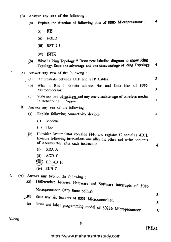
(a).Explain the function of following pins of 8085 Microprocessor:
(1). RD
View Solution
The RD pin is an active low signal used for reading data from the memory or I/O devices into the microprocessor.
Features:
- When RD is low, data is read from memory or I/O.
- It is synchronized with the system clock to ensure correct data retrieval.
- It enables the processor to fetch instructions or data. Quick Tip: The RD signal is crucial for fetching data from external devices or memory.
(2). HOLD
View Solution
The HOLD pin is used for external devices to gain control over the system's buses during DMA (Direct Memory Access) operations.
Features:
- It signals the microprocessor to relinquish control of the buses.
- Essential for transferring large amounts of data without processor intervention.
- The microprocessor responds by releasing the buses once HOLD is asserted. Quick Tip: HOLD is crucial for efficient data transfer in systems requiring DMA operations.
(3). RST 7.5
View Solution
RST 7.5 is a restart interrupt pin that triggers an interrupt service routine at vector address 0x003C.
Features:
- It is a software interrupt that can be invoked by external devices.
- Used for handling high-priority events in the system.
- Provides direct control over program flow during critical operations. Quick Tip: RST 7.5 is essential for responding to high-priority tasks quickly.
(4). INTA
View Solution
The INTA pin is used to acknowledge an interrupt request from an external device.
Features:
- It is used by the microprocessor to signal an interrupt request.
- When low, it indicates that an interrupt has been acknowledged.
- Ensures proper handling of interrupts during system operation. Quick Tip: The INTA pin is critical for managing interrupt-driven processes in microprocessor systems.
(b). What is Ring Topology? Draw neat labelled diagram to show Ring Topology. State one advantage and one disadvantage of Ring Topology.
View Solution
Ring Topology:
In a Ring Topology, each device is connected to two other devices, forming a ring-like structure. Data travels in one direction around the ring, passing through each device until it reaches the destination.

Advantage:
- Efficient for small networks and data is transmitted in one direction, reducing collisions.
Disadvantage:
- A failure in any device or connection can disrupt the entire network. Quick Tip: Ring Topology is more efficient for small networks but can be difficult to troubleshoot due to its dependency on every device in the network.
Question 3(A):
(a). Differentiate between UTP and STP Cables.
View Solution
Table for UTP and STP Differences with proper alignment
| UTP (Unshielded Twisted Pair) | STP (Shielded Twisted Pair) |
|---|---|
| 1. No Shielding – UTP cables do not have any shielding to protect against external interference. | 1. Shielding Present – STP cables have an additional shielding layer to protect from external interference. |
| 2. Lower Cost – UTP is cheaper due to the absence of shielding. | 2. Higher Cost – STP cables are more expensive because of the extra shielding material. |
| 3. Used for Shorter Distances – Best for shorter-range communication due to susceptibility to interference. | 3. Used for Longer Distances – STP cables are better for long-distance communication with minimal interference. |
(b). What is Bus? Explain address Bus and Data Bus of 8085 Microprocessor.
View Solution
Bus: A bus is a communication system that transfers data between different components of a computer or between computers. It allows multiple components to communicate with each other by transmitting data, instructions, and control signals.
% Address Bus of 8085 Microprocessor
Address Bus of 8085 Microprocessor:
The address bus is unidirectional, meaning it transmits data in one direction from the microprocessor to memory or I/O devices.
It carries the address of the memory or I/O device from which data is to be fetched or to which data is to be sent.
The 8085 microprocessor has a 16-bit address bus, meaning it can address up to 64KB (65536 locations) of memory.
% Data Bus of 8085 Microprocessor
Data Bus of 8085 Microprocessor:
The data bus is bi-directional, meaning it can transfer data in both directions: from memory to microprocessor or vice versa.
It is used to carry actual data being transmitted to/from the microprocessor.
The 8085 microprocessor has an 8-bit data bus, meaning it can transfer 1 byte of data at a time. Quick Tip: The address bus carries addresses, while the data bus carries actual data between components in the system.
(c). State any two advantages and any one disadvantage of wireless media in networking.
View Solution
Advantages of Wireless Media
Advantages of Wireless Media in Networking:
Mobility – Wireless media allows devices to move freely within a network without being restricted by cables.
Easy Installation – Wireless networks do not require physical cables, making installation easier and more flexible.
Disadvantage of Wireless Media
Disadvantage of Wireless Media in Networking:
Limited Range – Wireless media has a limited range, meaning the signal strength decreases with distance, making it less suitable for large-scale networks. Quick Tip: While wireless media offers flexibility and convenience, it is important to consider factors like range and security in designing wireless networks.
Question 3(B):
(a). Explain the following connectivity devices :
(1). Modem
View Solution
Modem:
A Modem (Modulator-Demodulator) is a device that converts digital data from a computer into analog signals, and vice versa, for transmission over phone lines or cable systems. It enables internet connectivity by encoding and decoding signals. Quick Tip: A modem is essential for connecting a computer or network to the internet, especially in areas where broadband is not available.
(2). Hub
View Solution
Hub:
A Hub is a basic networking device used to connect multiple devices in a Local Area Network (LAN). It operates at the physical layer of the OSI model and forwards data to all connected devices. However, it does not have the ability to filter or route the traffic, so all data is sent to every device connected to the hub. Quick Tip: While hubs are simple and inexpensive, they are largely replaced by more efficient devices like switches that can direct traffic more intelligently.
Question 3(B):
(b) Consider Accumulator contains FFH and register C contains 4DH. Execute
following instructions one after the other and write contents of Accumulator after
each instruction:
(1). XRA A
View Solution
The instruction XRA A performs a bitwise XOR operation between the Accumulator and register A.
Given that both the Accumulator and A contain FFH (1111 1111 in binary), the result of XOR operation will be:
FFH ⊕ FFH = 00H
After XRA A, the Accumulator contains: 00H. Quick Tip: XRA performs an XOR operation, and XORing a value with itself always results in zero.
(2). ADD C
View Solution
The instruction ADD C adds the contents of register C (which is 4DH) to the Accumulator.
At this point, the Accumulator is 00H, so the result of adding 4DH to 00H is: 00H + 4DH = 4DH
After ADD C, the Accumulator contains: 4DH. Quick Tip: The ADD instruction adds the contents of a specified register to the Accumulator, modifying only the Accumulator's value.
(3). CPI 4D H
View Solution
The instruction CPI 4D H compares the contents of the Accumulator with the immediate value 4DH. It subtracts the immediate value (4DH) from the Accumulator, but the result is not stored in the Accumulator. It only affects the flags.
Since the Accumulator is 4DH, subtracting 4DH from it results in 00H, and the Accumulator remains unchanged.
After CPI 4D H, the Accumulator contains: 4DH. Quick Tip: CPI instruction does not modify the Accumulator, it only updates the flags based on the result of the subtraction.
(4). SUB C:
View Solution
The instruction SUB C subtracts the contents of register C (4DH) from the Accumulator.
At this point, the Accumulator contains 4DH, and subtracting 4DH from it results in: 4DH − 4DH = 00H
After SUB C, the Accumulator contains: 00H. Quick Tip: SUB instruction subtracts the contents of a specified register from the Accumulator and stores the result in the Accumulator.
(a). Differentiate between Hardware and Software interrupts of 8085 Microprocessor. (Any three points)
View Solution
Difference between Hardware and Software Interrupts:
| Hardware Interrupts | Software Interrupts |
|---|---|
| Initiated by external hardware devices | Initiated by the program instructions |
| Takes place automatically when an interrupt occurs | Triggered explicitly by executing an interrupt instruction |
| Requires external hardware support (e.g., interrupt pins) | Does not require external hardware; it is initiated by software |
| Faster response time due to direct hardware signals | Slower response time since it depends on the program's instruction cycle |
| Examples: INTR, RST7.5, RST6.5, etc. | Example: SIM (Software Interrupt) in 8085 |
(b). State any six features of 8051 Microcontroller.
View Solution
Six Features of 8051 Microcontroller:
8-bit Processor: 8051 is an 8-bit microcontroller, which means it can handle 8 bits of data at a time.
4KB ROM (Read-Only Memory): It has built-in 4KB ROM for storing the program code.
128 Bytes RAM: 8051 has 128 bytes of RAM for data storage and temporary variables.
4 Parallel I/O Ports: It has 4 parallel input/output ports, each 8 bits wide, allowing interaction with external devices.
16-bit Timer/Counters: It contains two 16-bit timers/counters for precise time delays or counting operations.
Serial Communication Control: It supports full-duplex serial communication, enabling data transmission and reception over serial ports. Quick Tip: The 8051 microcontroller is widely used in embedded systems due to its versatile I/O capabilities, onboard memory, and serial communication features.
(c). Draw and label programming model of 80286 Microprocessor.
View Solution
The 80286 microprocessor has a 24-bit address bus and an 8-bit data bus. It uses segmentation and paging for memory management, and its programming model consists of multiple registers.
 Quick Tip: The 80286 microprocessor introduced segmentation, which allows the system to use larger memory spaces efficiently compared to earlier microprocessors.
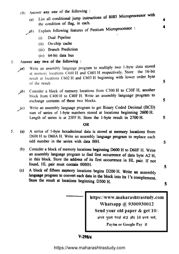
(a). List all conditional jump instructions of 8085 Microprocessor with the condition of flag in each.
View Solution
The 8085 microprocessor has the following conditional jump instructions along with their corresponding flag conditions:
| Instruction | Condition of Flag |
|---|---|
| JZ (Jump if Zero) | Zero Flag (Z) = 1 |
| JNZ (Jump if Not Zero) | Zero Flag (Z) = 0 |
| JC (Jump if Carry) | Carry Flag (C) = 1 |
| JNC (Jump if No Carry) | Carry Flag (C) = 0 |
| JP (Jump if Positive) | Sign Flag (S) = 0 |
| JM (Jump if Minus) | Sign Flag (S) = 1 |
| JPE (Jump if Parity Even) | Parity Flag (P) = 1 |
| JPO (Jump if Parity Odd) | Parity Flag (P) = 0 |
(b). Explain the feature of Dual Pipeline in Pentium Microprocessor:
(1). Dual Pipeline
View Solution
Dual Pipeline: The Pentium microprocessor uses a dual pipeline architecture, where two instructions are fetched and executed in parallel. This increases instruction throughput and overall processing speed, making the processor more efficient in handling tasks simultaneously. Quick Tip: Dual pipelines allow the processor to handle two instructions at once, reducing the time spent on each instruction and improving performance.
(2). On-chip Cache
View Solution
On-chip Cache: The Pentium microprocessor incorporates an on-chip cache memory, which stores frequently accessed data. This reduces the time needed to retrieve data from the slower main memory, improving the speed and performance of the processor. Quick Tip: On-chip cache stores frequently accessed data locally, reducing memory access time and improving processor speed.
(3). Branch Prediction
View Solution
Branch Prediction: Pentium microprocessor uses branch prediction techniques to guess the outcome of a branch instruction before it is fully executed. This allows the processor to continue executing subsequent instructions without waiting for the branch to be resolved, improving overall performance. Quick Tip: Branch prediction reduces wait times by allowing the processor to guess the direction of branches, leading to smoother instruction execution.
(4). 64-bit Data Bus
View Solution
64-bit Data Bus: The Pentium microprocessor has a 64-bit data bus, allowing it to transfer data in 64-bit chunks. This improves the processor’s ability to handle large amounts of data and perform faster data processing, leading to better overall performance. Quick Tip: A 64-bit data bus enables faster data transfers and allows the processor to handle more data in parallel, boosting performance.
(a). Write an assembly language program to multiply two 1-byte data stored at memory locations C600 H and C601 H respectively. Store the 16-bit result at locations C602 H and C603 H beginning with lower order byte of the result.
View Solution
    MVI H, C6    ; Load memory location C600 H into HL pair
    MOV L, M     ; Move contents of C600 H to L register
    INX H        ; HL = C601 H
    MOV H, M     ; Move contents of C601 H to H register
    MOV A, L     ; Load A with the first byte
    MUL H        ; Multiply L by H (multiplication result in AL)
    MOV C, A     ; Store result (lower byte) in C602 H
    MOV D, B     ; Store result (higher byte) in C603 H
Quick Tip: Use `MOV` and `INX` instructions for memory manipulation, and `MUL` for multiplication. Don't forget to store both high and low bytes of the result.
(b). Consider a block of memory locations from C300 H to C30F H, another block from C400 H to C40F H. Write an assembly language program to exchange contents of these two blocks.
View Solution
    MVI H, C3    ; Load C300 H into HL pair
    MOV L, M     ; Move contents of C300 H to L
    INX H        ; HL = C301 H
    MOV H, M     ; Move contents of C301 H to H
    MVI D, C4    ; Load C400 H into DE pair
    MOV E, M     ; Move contents of C400 H to E
    INX D        ; DE = C401 H
    MOV D, M     ; Move contents of C401 H to D
    ; Repeat the process for entire block exchange
Quick tip: Using ‘MOV‘, ‘INX‘, and ‘MVI‘ ensures you can move data between different memory
locations efficiently.
(c). Write an assembly language program to get Binary Coded Decimal (BCD) sum of series of 1-byte numbers stored at locations beginning 2600 H. Length of series is at 25FF H. Store the 1-byte result in 2700 H.
View Solution
MVI H, 26 ; Load 2600 H into HL pair
MOV L, M ; Move data to L register
INX H ; HL = 2601 H
MOV A, M ; Load A with 2600 H value
ADD A, L ; Add next number
MOV M, A ; Store result back in memory
; Repeat the process for series length
Quick Tip: For BCD addition, use the `ADD` instruction and ensure proper handling of carry and overflow.
(a).A series of 1-byte hexadecimal data is stored at memory locations from D600 H to D60A H. Write an assembly language program to replace each odd number in the series with data 00H.
View Solution
MVI H, D6 ; Load memory location D600 H into HL pair
MOV L, M ; Move contents of D600 H to L register
INX H ; HL = D601 H
MOV H, M ; Move contents of D601 H to H register
MOV A, L ; Load A with the first byte
ANI 01H ; AND the accumulator with 01H to check if odd
JZ EVEN ; If result is zero, it is an even number, jump to EVEN
MVI M, 00H ; Replace odd number with 00H if odd
EVEN:
INX H ; Move to the next memory location
MOV L, M ; Move contents to L for checking next byte
MOV A, M ; Check next byte
JNZ LOOP ; If there are more bytes, continue loop
HLT ; Halt when done
Quick Tip: Use the `ANI` instruction to check for odd numbers (bitwise AND with 01H). You can skip changing even numbers and handle only odd ones.
(b). Consider a block of memory locations beginning D600 H to D60F H. Write an assembly language program to find first occurrence of data byte A2 H in this block. Store the address of its first occurrence in HL pair. If not found, HL pair must contain 0000H.
View Solution
    MVI H, D6    ; Load memory location D600 H into HL pair
    MVI L, 00    ; Clear L register
    MOV A, M     ; Load the first byte into A
    INX H        ; Increment HL to D601 H
    MOV L, M     ; Move data of D601 H to L register
    MOV A, L     ; Load A with D601 H data
    CMP A2H      ; Compare with A2H
    JZ FOUND     ; If A2H is found, jump to FOUND
    INX H        ; Move to next byte
    MOV L, M     ; Move data into L register
    MOV A, L     ; Compare again
    JNZ LOOP     ; Continue loop until found or end
FOUND:
    MOV H, L     ; Store found address in HL
    MOV L, 00H   ; If not found, store 0000H
(c). A block of fifteen memory locations begins D200 H. Write an assembly language program to convert each data in the block into its 1’s complement. Store the result at locations beginning D300 H.
View Solution
    MVI H, D2    ; Load memory location D200 H into HL pair
    MOV L, M     ; Move data to L register
    INX H        ; HL = D201 H
    MOV H, M     ; Move data to H register
    COM A        ; Complement the data in the A register
    MOV M, A     ; Store 1’s complement at D200 H
    INX H        ; Move to next location
    MOV L, M     ; Move to L for next byte
    MOV A, M     ; Complement the next byte
    MOV M, A     ; Store the complement at the next location
    LOOP:        ; Repeat for 15 bytes in total
    JNZ LOOP     ; Loop until all bytes are converted


*The article might have information for the previous academic years, please refer the official website of the exam.